POSEIDON aims to fabricate a demonstrator on-chip light source for data transmission or sensing on a PIC within a short time scale. After successfull integration, lasers can be created by coupling the emitters to nanophotonic resonators. The long-term vision of POSEIDON goes far beyond the creation of on-chip light sources. The aim is to establish a manufacturing platform for generic PICs consisting of monolithically integrated active colloidal components (light sources and detectors), combining silicon photonics and CMOS electronics. The benefits of POSEIDON can be quantum leaps in data center energy efficiency and network performance, enabled by the project targeting the usual Datacom wavelengths, and cheap yet powerful optical sensors.
To reach this goal, POSEIDON works on integrating efficient and power
ul colloidal light sources into silicon-based waveguides. Success of the project spans the entire process chain, from the theoretical understanding of emission enhancement, via the synthesis, self-assembly and integration of colloidal light sources, to the design of complete devices.
Theory of Colloidal Assembly and Nanophotonics
POSEIDON seeks to design and implement a hybrid emitter-nanoantenna building block to be integrated on a chip as an efficient light emission device. An important aspect of the design of such emitter-nanoantenna building block is to optimize the intense field enhancements in the proximity of the nanoantennas where light emitters are deposited and efficiently excited. This occurs in the hot spots of plasmonic nanoantennas as the ones shown in the left figure below. The quantum yield of the emitter in a particular hot spot will eventually determine the final light emission probability of the hybrid system.
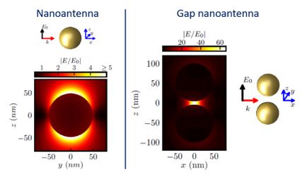
The unique behavior of colloids at liquid interfaces provides exciting opportunities to design the assembly of colloids into dimensionally confined structures. In this project we will exploit the strong electrostatic and surface tension forces present in interfacial environments to assemble colloids into the desired nanoantenna structures, seen in the right figure above. We will also use interfacial curvature as an additional handle to direct colloidal assembly
Synthesis and Self-assembly of Colloidal Light Sources
Polymers are a suitable class of materials for encapsulation of sensitive components, such as metallic and semiconductor nanoparticles, in order to protect them from detrimental environmental influences like humidity. For this purpose, various polymerization techniques are employed and optimized for the preparation of colloidal particles to embed other nanoparticles. These polymeric particles can be further subjected to colloidal assembly processes to localize them on specific locations on structured surfaces. Polymer chains with well-defined architecture and functional groups are synthesized by advanced polymerization techniques in order to modify the metallic and semiconductor nanoparticles at their surface.
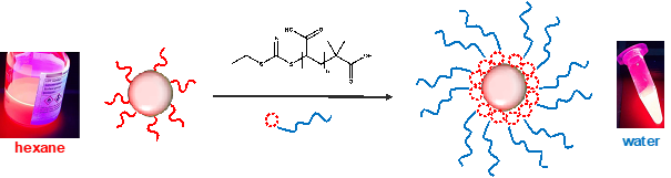
The image above shows a semiconductor nanoparticle, which is initially hydrophobic and dispersed in hexane. After deposition of sulfur-containing poly(acrylic acid) chains to the surface the nanoparticle can be suspended in water.
Metal nanoparticles can be synthesized in various shapes and sizes, by means of wet/colloid chemistry methods. The surface chemistry of the resulting nanoparticles can be tuned by either ligand exchange or seeded-growth of another material, such as metal oxide shells.
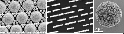
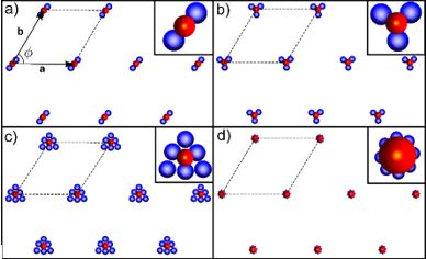
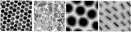
If sufficiently uniform in size, colloidal particles can be self-assembled into defined superstructures. The resulting structures can be controlled by the process conditions, the interactions between the particles, or the choice of a suitable confinement. Self-assembled structures that can be formed include periodic arrays of particles, colloidal clusters with defined structure and symmetry, dimers and oligomers, or two-dimensional lines.
Integration of Colloidal Light Sources and Electrical Contacting
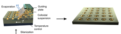
Different fabrication processes can be used to trap and guide the self-assembly of colloidal particles into defined surface areas, for example exploiting defined surface topographies, using wettability contrasts, or localized attractive surface chemistries.
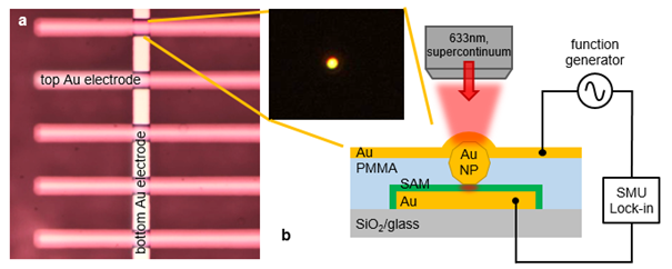
Using self-assembly in patterned contact arrays, colloids with nanogaps between the metal nanoparticles can be integrated. The resulting electrical drive can produce light emission in the plasmonic nanogaps which can be efficiently harvested.
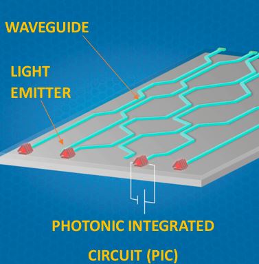
Integration of Light Emitters into Photonic Integrated Circuits
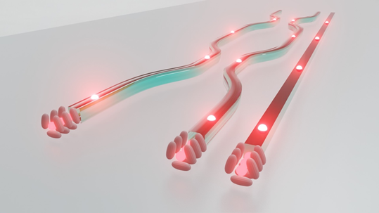
The light emitted by the assembled colloidal particles is efficiently coupled into silicon based photonic waveguides can directly be used by the photonic circuitry. This enables applications such as low-cost sensing, point-of-care medicine and many more.